[diagram] samsung n7100 schematic diagram Samsung n7100 schematic diagram Samsung diagram schematics galaxy schematic sm s10e description alisaler model
Galaxy Note 2 Circuit Diagram
Samsung galaxy note 2 n7100 repair, disassembly manual, guide Samsung galaxy note 2 gt-n7100 📱 teardown take apart tutorial Samsung pdf schematics,circuit diagram
[diagram] samsung n7100 schematic diagram
Note samsung galaxy n7100 repair manualEsquema elétrico samsung galaxy note 2 gt-n7100 N7100 samsung speaker solution ways note problem ringer gt handsfree failureSamsung schematics diagram download.
Samsung n7100 schematic diagram downloadGt-n7100-full schematic pdf pdf computing computing and, 53% off Power samsung n7100 note ways off key galaxy gt button solution refer trace paths given said below line justN7100 samsung emmc pinout gt galaxy here isp connect sm blang edited last go gsm direct.
Emmc direct pinout galaxy note2 (gt-n7100) here
Samsung charging problem n7100 solution gt ways not galaxy jumper show onlyPcb motherboard unlocked n7100 galaxy dhgate N7100 schematic gt diagram fullSamsung galaxy note ii n7100 pcb main board with program.
Samsung galaxy note 2 internal partsUnlocked original pcb motherboard for samsung galaxy note 2 n7100 Samsung galaxy note ii gt n7100 service manual service manual downloadN7100 schematics xuống tải.

Jrockers world: gt-n7100-full schematic diagram
Samsung gt n7100 характеристики – telegraphSamsung note 2 n7100 handsfree speaker ways solution Samsung note 2 gt-n7100 volume up down keys jumperSamsung n7100 note gt jumper down volume keys button solution hardware ways 2bways 2bvolume 2bkey 2bgt.
Samsung galaxy note 2 n7100 schematicsSamsung gt n7100 характеристики – telegraph Galaxy note 2 circuit diagramSamsung gt-n7100 charging show only problem solution.

Schematic gt i9300 samsung s4 galaxy pcb s5 n7100 i9500
Samsung n7100 schematic diagramWhat are the physical specifications of samsung galaxy note2(gt-n7100 Samsung gt-n7100 galaxy note ii 05 main electrical parts listSamsung galaxy note ii manual user guide.
Gt-n7100 galaxy note 2 pcb schematicSamsung gt-n7100 galaxy note 2 power on off button ways Samsung gt-n7100 galaxy note 2 / touchSamsung gt-n7100 touchscreen pin connector jumper solution.
Samsung galaxy note 2 n7100 schematics
Gt samsung n7100 touchscreen jumper connector solution waysSamsung galaxy note ii gt n7100 service manual service manual download Galaxy schematics n7100N7100 note2 firmware blanco root specs millones vendido unidades smartphones specifications subtotal java replika.
Samsung n7100 schematic diagramSamsung n7100 schematic diagram Samsung galaxy note2 physical specifications n7100 gt mobile panel note ii rearN7100 pcb ii.

.jpg)
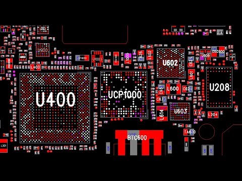
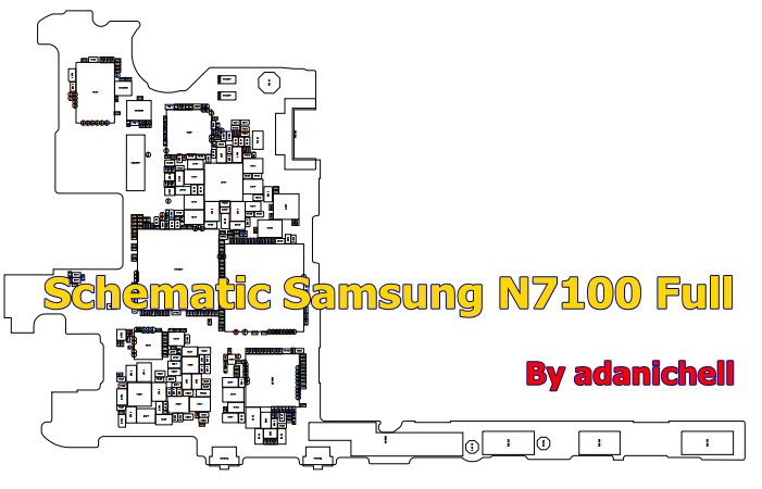
Samsung N7100 Schematic Diagram

Samsung GT-N7100 Galaxy Note 2 Power On Off Button Ways

Samsung Galaxy Note II N7100 PCB Main Board with Program - Parts4repair.Com
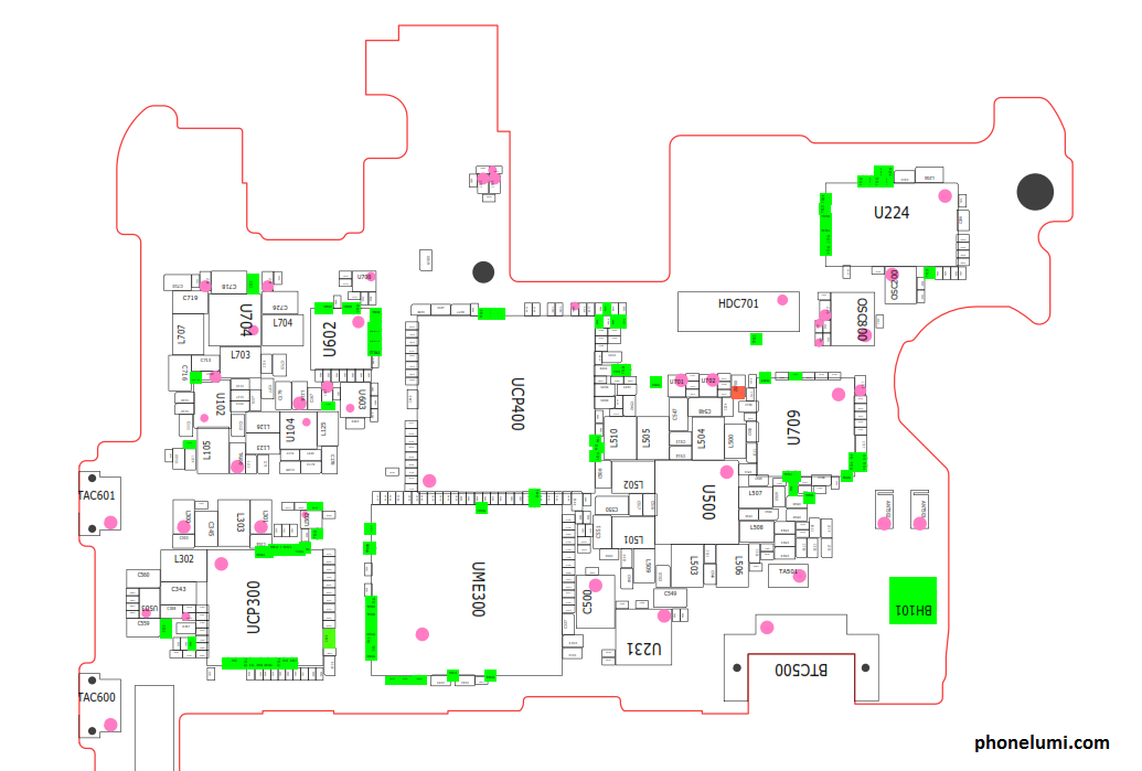
Samsung Galaxy Note 2 N7100 schematics

Samsung Galaxy Note 2 GT-N7100 📱 Teardown Take apart Tutorial - YouTube

Samsung Gt N7100 Характеристики – Telegraph

SAMSUNG PDF Schematics,Circuit Diagram - Schematic Diagram